Types of electronic components, pn junction connection and uses
Most electronic components & devices are made of semiconductors which are known to be sensitive to environmental conditions such as light, heat, pressure, radiation and chemical pollution, That is why they are used as sensors or means for measuring external stimuli, Electronic components & devices are the building blocks for all the electronic systems.
Types of electronic components
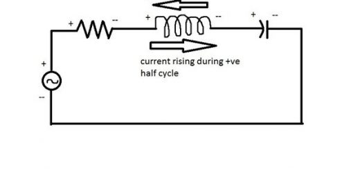
- Simple components: Such as resistor (R), induction coil (L), capacitor (C).
- Complex components: such as pn junction (diode) and transistor.
- Specialized components: such as optoelectronic and current control devices.
The pn junction
Structure: It consists of n-type crystal and p-type crystal.
Explaining the way of working:
In the p-type crystal, the concentration of holes (p) is greater than the concentration of electrons (n), while the concentration of holes in the n-type crystal is lower than the concentration of electrons.
Some holes diffuse from the p-type region to the n-type region, Also, some electrons diffuse from the n-type region (high concentration for electrons) to the p-type region (low concentration for electrons) which is called diffusion current.
The transfer of some electrons from the n-type region does not cover all the holes from the positive donor ions and the transfer of some holes from p-type region does not cover all the electrons from the negative acceptor ions, This results in a middle region free of charge called transition (depletion) region with positive ions on one side and negative ions on the other side.
When the crystal of n-type loses some of its electrons, it acquires a positive voltage while the crystal of p-type acquires negative voltage due to transferring electrons to it, thus an electric field is set up and its direction from n-crystal (positive voltage) to p-crystal (negative voltage), that generates electric current called drift current which is opposite to the diffusion current.
By continuous transferring of electrons and holes from high concentration to low concentration, the potential difference between the two crystals increases up to a certain value where the diffusion current = Drift current where there is no transferring of electrons from n to p and the potential difference is called the voltage barrier of pn junction.
Diffusion current is the current that resulted from the diffusion of positive holes from region (p) to region (n) and diffusion of electrons from region (n) to region (p) at the contact position of the two crystals, The depletion (transition) region is the region which does not contain charge carriers but at its two sides the crystal (n) and crystal (p) in pn junction.
Drift current is the current which is resulted from the internal electric field between positive ions in the n region and negative ions in the p region at the two sides of the contact region of the pn junction and it is opposite to the diffusion current.
The voltage barrier of pn junction is the least potential difference at the two sides of the p and n contact position which is enough to prevent the diffusion of more holes and free electrons to the low-concentration region.
When the voltage barrier of pn junction = 0.3 V, It means that the least potential difference at the two sides of the p and n contact position which is enough to prevent the diffusion of more holes and free electrons to the low concentration region = 0.3 V.
Connection of pn junction
The pn junction is connected by two methods in the electric circuit:
The forward bias of pn junction
P-type crystal is connected to the positive terminal of the battery and n-type crystal is connected to the negative terminal of the battery, The direction of the external field (due to the battery) is opposite to the direction of the internal field in the transition region and therefore, it weakens it.
The voltage of pn junction becomes less than the barrier voltage, the Thickness of the transition region decreases, (holes and electrons repel with the poles of the battery and move closer to the separating surface), Resistance of the junction (R) is small, High-intensity electric current passes through the junction.
Reverse bias of pn junction
P-type crystal is connected to the negative terminal of the battery and n-type crystal is connected to the positive terminal of the battery, The direction of the external field (due to the battery) is in the same direction of the internal field in the transition region and therefore, it strengthens it.
Voltage of pn junction becomes greater than the barrier voltage, Thickness of the transition region increases, (holes and electrons attract with the poles of the battery and move far away from the separating surface), Resistance of the junction (R) is large, The electric current intensity is very weak almost vanished, I = 0.
Uses of pn junction
- Used as a switch: When the pn junction is connected in the forward direction, it allows the flow of the electric current in the circuit, thus it acts as a closed switch, While when it is connected in the reverse direction it does not allow the current to flow through the circuit and it acts as an opened switch.
- Rectification of alternating current: It means converting the alternating current (which is changeable in intensity and direction) into a unidirectional current which is used in charging the car battery and the cell phone, We can convert the AC current into DC current by using many pn junctions.
Ohmmeter can be used to make sure that the pn junction is functioning, such that the diode has a small resistance in the forward direction and a large resistance in the reverse direction, Ohmmeter can be used to differentiate between the pn junction and the ohmic resistance:
- In case of pn junction: the reading of ohmmeter is very large in the forward direction and very small in the reverse direction.
- In case of an ohmic resistance: the reading of ohmmeter does not change if the direction of the current is reversed.
We can compare between the pn junction and the ohmic resistance:
Pn junction consists of two attached crystals n and p, The charge carriers are free electrons or holes, The electric current intensity passes in one direction and does not pass in the reverse direction, By increasing the temperature, the resistance decreases and the conductivity increases.
Ohmic resistance consists of a coil of wire of suitable resistivity such as tungsten or nichrome, The charge carriers are free electrons, The electric current intensity passes in two directions, By increasing the temperature, the resistance increases and the conductivity decreases.
Electronic tuning
To tune up a TV or radio onto a certain station, we need to adjust the value of a capacitor to set the frequency of the receiver to the frequency of the selected broadcast station, this condition is called resonance.
In modern receivers, the capacitor is replaced by a reverse-biased pn junction, The width of the transition region increases with increasing reverse bias, The increase of the width of the transition region means an increase of the fixed ionic charge on both sides of the transition region with reverse voltage, This is tantamount to capacitor action.
Thus, we can change the value of the capacitor by controlling the reverse voltage, This is called electronic tuning (and the device is called a varactor).
Pure semiconductor crystal & ways of increasing the conductivity of semiconductors
Transistor types, structure (pnp transistor & npn transistor)